Tech Insights: A behind-the-scenes look at rolling out new GPU resources for NZ researchers
Over the past few months, there has been a lot of excitement at NeSI following the arrival of eight new A100 GPUs. On 20 May, we invited research groups using machine learning applications to begin accessing these advanced GPU capabilities (if this applies to you, contact Support to learn more!). It was an exciting culmination to months of preparation and technology validation activities.
That pre-launch testing phase is often a story that goes untold, but at NeSI it’s an important part of how we’re actively developing, testing, and problem-solving technology to support research and researcher's evolving needs.
So, we’ve decided to share some of our ‘behind-the-scenes' experiences with rolling out the A100s as a round of ‘Tech Insights’ blog posts. Over the series, we’re going to talk about our journey with these incredible pieces of hardware and share what we've learned along the way.
This opening post shares insights from our first tasks with the A100s: thermal and internal software tests. In future posts, we’ll explore user tests we conducted in the spaces of deep learning and molecular dynamics code. (For a higher-level view of how this all fits into our broader support of data science in New Zealand, have a read of this earlier news item.)
Cards installation and thermal testing
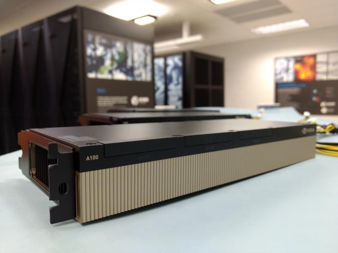
First, what does an A100 card look like? If you are used to GPUs for gaming, you might be a little bit disappointed: the A100 are nice looking black bricks. No shiny multi-color LEDs to get the party started! But to be fair, in the darkness of an HPC node’s internal workings, no one will see you glowing.
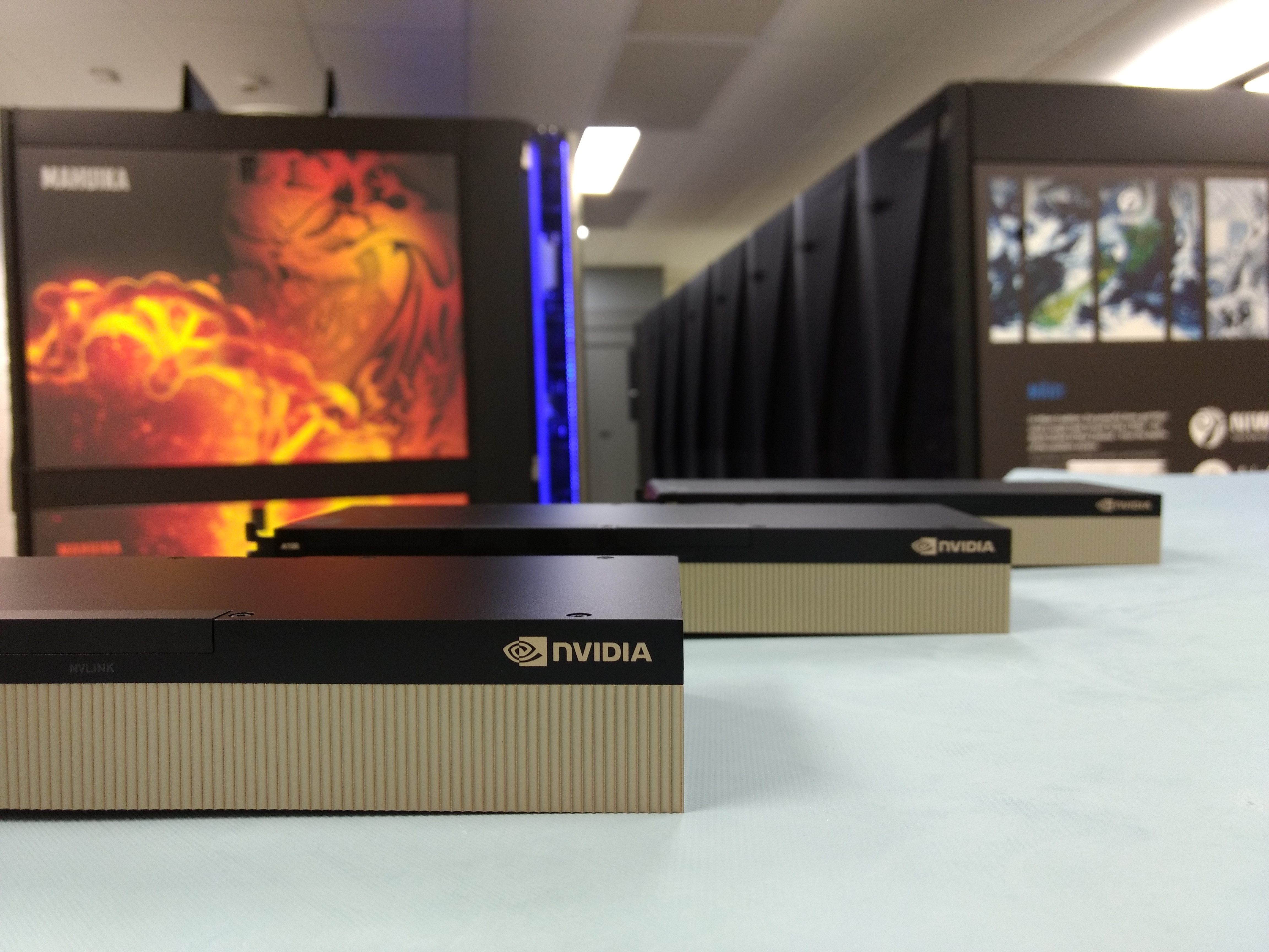
Regarding the specs, we opted for 40GB PCIe cards. We split them among six nodes:
two nodes with two GPUs each, and
four nodes with one GPU each.
The power requirements of these little monsters are quite high (250W Watts per GPU!) and, as we will see later, the cooling requirements are too.
Unfortunately, the hosting nodes are existing 2U servers without appropriate internal space to mount the cards next to each other. Sadly this makes it impossible to put an NVLink Bridge between the two cards for now. But watch this space - we will be moving them into new hardware sooner than you might expect...
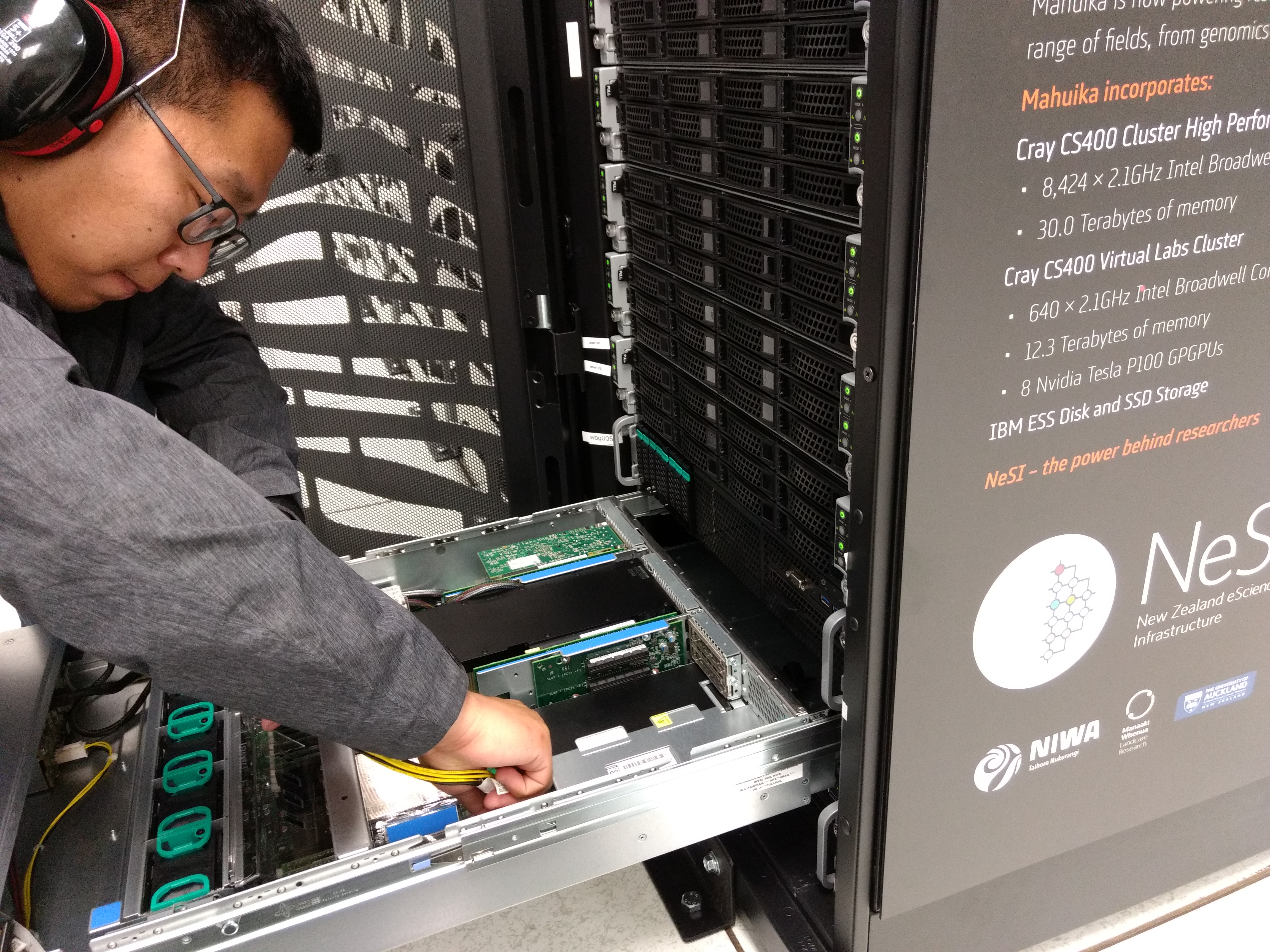
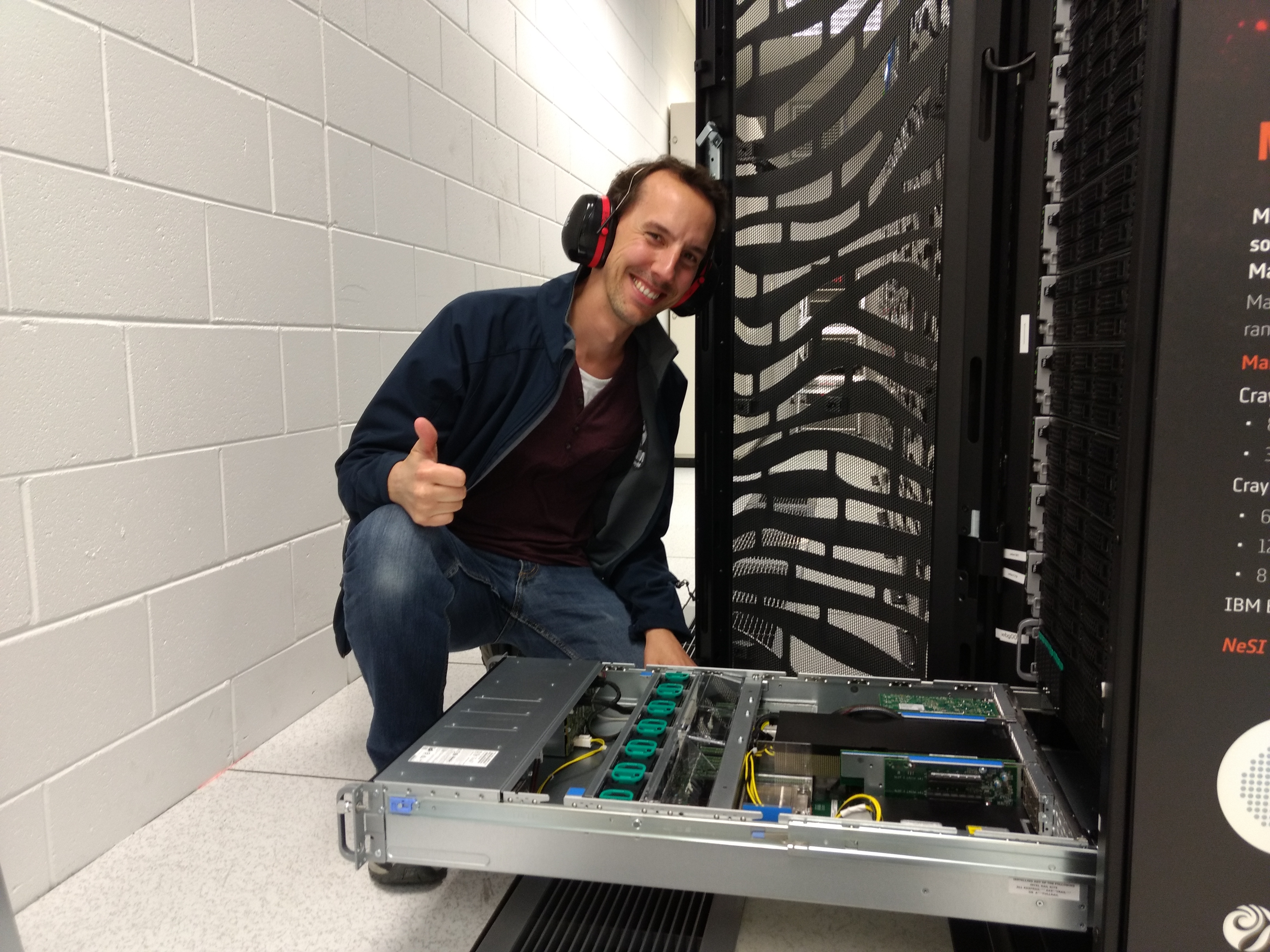
So now we have them up and running. What else do we need to start playing with them?
Well, we intend to use them as much as possible, 24/7 if possible, so we needed to ensure reliability of the hardware, i.e. so it doesn’t literally catch on fire, or more realistically it does not shutdown under heavy load. This is what we call the stress tests: we run a program on the GPU that will make use of it as much as possible for a long period of time.
We used the gpu-burn program as it has advantages of being easy to use, capable of testing multiple GPUs at a time, and enabling use of Tensor Cores (computing units especially performant for AI workloads). Under the hood, it fills the GPU with matrix multiplication operations using cuBLAS. To emulate a worst case scenario, we also used the Linux command stress at the same time to push the 36 physical cores of the hosting node to their limit.
After 10 hours at this regime, good news, the system was still working! However when we looked more closely at the temperature and performance graphs, something caught our eye. Below you can see one of these graphs, where GPU1 is already warm due to a previous five-hour test and GPU0 starts from a cooler state as it was not involved in this previous test.
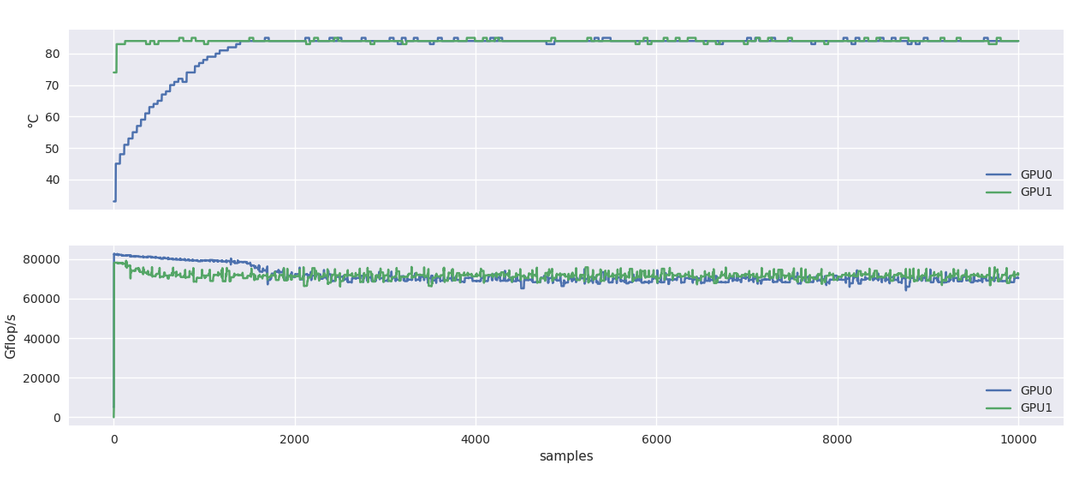
You can notice that the performance for GPU0 peak at 80 TFLOPS before going down to about 75 TFLOPS, at the same level of the already warm GPU1. This decrease in performance coincides with the temperature rising at 85C.
Note: I would not focus too much here on the raw performance numbers. These are about half of what the specifications say (156 TFLOPS for single precision TF32 use case) but other indicators such as nvidia-smi showing the full utilization of the card, we assume that it is likely a multiplicative factor missing here.
What happens here is software triggered thermal throttling, which means that the card will decrease its clock speed if a certain temperature is reached. In the present case, the limit is 85C. As a side note, the A100 card will shutdown at 95C.
That is not very good news, and subsequent tests revealed that it is happening even with lower workloads (only one GPU involved in the test and no load on the CPUs). Fortunately, our onsite HPE engineer Tony Racho found a solution: cranking up the fan speed. This was enough to lower the peak temperature by few degrees and turn off the thermal throttling!
Internal code testing - let’s check what we have in-house
To test the GPUs some more, we revisited an OpenACC code for computing the log-determinant of a matrix, written by Damien Mather (University of Otago), which we had worked on in a previous Consultancy project. This code supports parallel computing through MPI, can run with or without GPUs and across multiple nodes, thus we were able to compare Māui nodes (without GPUs), our older P100 GPUs, and the new A100 GPUs.
This code relies on Fortran, MPI and OpenACC. Thus, in order to compile it to run on GPUs, we used the NVIDIA HPC SDK (previously known as the PGI compilers), which is available on Mahuika in the NVHPC environment module, along with Intel MPI.
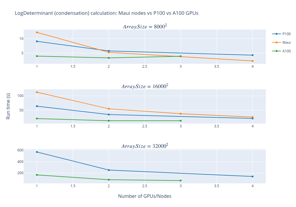
The graph below shows that an A100 performed about 3x faster than a P100 and a single A100 gave about the same performance as four full Māui nodes (160 cores). Simulations with one or two GPUs were run on a single node while the simulation with three GPUs was across three nodes with one GPU per node. For smaller matrices, running on more GPUs is not really beneficial as the communication costs begin to dominate (particularly when running across three nodes).
Another benchmark code we used to evaluate the qualities of the A100 is the FiDiBench benchmark developed by one of our Research Software Engineers (RSEs), @Alexander Pletzer. The FiDiBench benchmark applies finite difference stencils to advect a bubble in 3D space. The code exhibits communication patterns that are representative of finite element, finite difference and finite volume codes. Examples of such codes can be found in climate science, fluid dynamics, and many areas of physics. FiDiBench is also very flexible, the problem size can be made arbitrarily large to suit the benchmark.
We had an OpenACC version of the code that was running on the P100 GPUs, which required no modification to run on the A100 except for the building step. Apart from two blasts of communication, at the beginning and end of the computation, all the data reside on the GPU for the duration of the calculation.
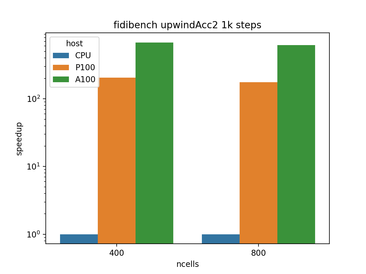
The calculation runs a staggering 700x faster on the A100 compared to a single Mahuika CPU core and 3.5x faster on the A100 compared to the P100. This demonstrates the potential of P100 and A100 GPUs to accelerate simulation codes.
Note: FiDiBench was also very helpful to diagnose throttling issue on the A100.
The last piece of code we will examine in this post is another code optimized as part of another Consultancy project, the Quasi‐equilibrium Tropical Circulation Model, developed by Dr. Gilles Bellon (University of Auckland).
This software already supported offloading computations to a GPU, using the cuBLAS library to perform linear matrix multiplications to solve the Poisson equation. Compared to the old P100 GPUs, we observed a very modest speedup, plateauing at 1.15x for this part of the code.
This result can be explained by the fact that the code is actually spending only 20% of its runtime on the GPU, so any difference between P100 and A100 speed will be marginally affecting the overall runtime. Additionally, using the Arm MAP profiler and zooming on the part of the code that is executed on the GPU revealed that all the time classified as GPU related actually involved copying data from the device to host (cuMemcpyDtoH_v2 function), so the compute speed of P100 vs. A100 won’t matter here. While not great, these results are a good teaching experience about where and when using a GPU makes more sense.

Conclusion
In this first part of our A100 Tech Insights series, we discussed our first internal tests, which let us build confidence that the base of our software stack was in place for some bigger tests. They also reminded us that GPUs can only give their best if used effectively, minimizing the transfers vs. compute time.
We also shared a few examples that demonstrate our new A100 GPU capability and how it fares compared to the older P100 GPUs. Whether your code might benefit from running on the A100 will ultimately depend on: (1) the cost of transferring data between CPU and GPU and (2) the proportion of time spent spent on the CPU vs the GPU. In the best case scenario, code can run several orders of magnitudes faster on the GPU compared to a single CPU and the A100 was found to be 3.5X faster than P100. Your mileage may vary.
This post explored the hot part of the installation, namely how to make sure your GPU will reliably work for hours without setting your HPC on fire. Stay tuned for the next instalments of our A100 Tech Insights, they will be cool!
If you are interested in learning more about these new GPU resources and whether they would be of use to your project, please contact NeSI Support.
